
 United Kingdom
 France
 Germany
 Netherlands
 Sweden
 USA
USA
 Italy
Italy
 Spain
Spain
More From Contributor


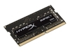


HyperX Impact 8GB DDR4 2400MHz SODIMM Memory
HyperX Impact 8GB DDR4 2400MHz SODIMM Memory HyperX HX424S14IB/4 is a 512M x 64-bit (4GB) DDR4-2400 CL14 SDRAM (Synchronous DRAM) 1Rx8, memory module, based on eight 512M x 8-bit DDR4 FBGA components. Each module supports Intel Extreme Memory Profiles (Intel XMP) 2.0. This module has been tested to run at DDR4-2400 at a low latency timing of 14-14-14 at 1.2V. Additional timing parameters are shown in the PnP Timing Parameters section below. The JEDEC standard electrical and mechanical specifications are as follows: PnP JEDEC TIMING PARAMETERS: JEDEC/PnP: DDR4-2400 CL14-14-14 @1.2V DDR4-2133 CL13-13-13 @1.2V XMP Profile 1: DDR4-2400 CL14-14-14 @1.2V FEATURES Power Supply: VDD = 1.2V Typical VDDQ = 1.2V Typical VPP - 2.5V Typical VDDSPD = 2.25V to 3.6V On-Die termination (ODT) 16 internal
banks; 4 groups of 4 banks each Bi-Directional Differential Data Strobe 8 bit pre-fetch Burst Length (BL) switch on-the-fly BL8 or BC4(Burst Chop) Height 1.18” (30.00mm) SPECIFICATIONS CL(IDD) 14 cycles Row Cycle Time (tRCmin) 46.75ns (min.) Refresh to Active/Refresh Command Time (tRFCmin) 260ns (min.) Row Active Time (tRASmin) 29.125ns (min.) Maximum Operating Power TBD W* UL Rating 94 V - 0 Operating Temperature 0oC to +85oC Storage Temperature -55oC to +100oC *Power will vary depending on the SDRAM used.
banks; 4 groups of 4 banks each Bi-Directional Differential Data Strobe 8 bit pre-fetch Burst Length (BL) switch on-the-fly BL8 or BC4(Burst Chop) Height 1.18” (30.00mm) SPECIFICATIONS CL(IDD) 14 cycles Row Cycle Time (tRCmin) 46.75ns (min.) Refresh to Active/Refresh Command Time (tRFCmin) 260ns (min.) Row Active Time (tRASmin) 29.125ns (min.) Maximum Operating Power TBD W* UL Rating 94 V - 0 Operating Temperature 0oC to +85oC Storage Temperature -55oC to +100oC *Power will vary depending on the SDRAM used.


Product Description
Reviews/Comments
Add New
Vouchers
No voucher codes found.
Do you know a voucher code for this product or supplier? Add it to Insights for others to use.
Do you know a voucher code for this product or supplier? Add it to Insights for others to use.
 Denmark