
 United Kingdom
 France
 Germany
 Netherlands
 Sweden
 USA
USA
 Italy
Italy
 Spain
Spain
More From Contributor


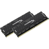

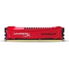


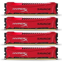
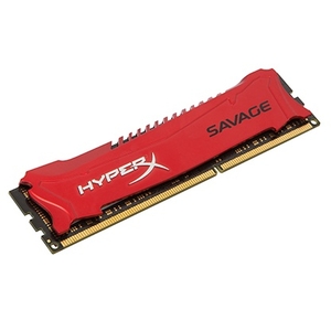
HyperX Savage 32GB (4x8GB) 1866MHz DDR3 Non-ECC 240-Pin CL9 DIMM PC
Memory Module
... FBGA components per module. Each module kit supports Intel XMP (Extreme Memory Profiles). Total kit capacity is 32GB. Each module has been tested to run at DDR3-1866 at a low latency timing of 9-10-11 at 1.5V. The SPDs are programmed to JEDEC standard latency DDR3-1600 timing of 11-11-11 at 1.5V. Each 240-pin DIMM uses gold contact fingers. Features JEDEC standard 1.5V (1.425V ~ 1.575V) Power Supply VDDQ = 1.5V (1.425V ~ 1.575V) 800MHz fCK for 1600Mb/sec/pin 8 independent internal banks Programmable CAS Latency: 11, 10, 9, 8, 7, 6 Programmable Additive Latency: 0, CL - 2, or CL - 1 clock 8-bit pre-fetch Burst Length: 8 (Interleave without any limit, sequential with starting address '000' only), 4 with tCCD = 4 which does not allow seamless read or write [either on the fly
using A12 or MRS] Bi-directional Differential Data Strobe Internal (self) calibration: Internal self calibration through ZQ pin (RZQ: 240 ohm ± 1%) On Die Termination using ODT pin Average Refresh Period 7.8us at lower than TCASE 85°C, 3.9us at 85°C TCASE 95°C Asynchronous Reset PCB: Height 1.18 inch (30mm), double sided component Extra Info Memory Size: 32768MB Module Size: 8192MB Memory Type: DDR3 Memory Package: DIMM Pin Configuration: 240 pins Main Colour: Red
using A12 or MRS] Bi-directional Differential Data Strobe Internal (self) calibration: Internal self calibration through ZQ pin (RZQ: 240 ohm ± 1%) On Die Termination using ODT pin Average Refresh Period 7.8us at lower than TCASE 85°C, 3.9us at 85°C TCASE 95°C Asynchronous Reset PCB: Height 1.18 inch (30mm), double sided component Extra Info Memory Size: 32768MB Module Size: 8192MB Memory Type: DDR3 Memory Package: DIMM Pin Configuration: 240 pins Main Colour: Red
%201866MHz%20DDR3%20Non-ECC%20240-Pin%20CL9%20DIMM%20PC%20Memory%20Module "Pin It")
Product Description
Reviews/Comments
Add New
Intelligent Comparison
Archived Product

HyperX SAVAGE 16GB (2 X 8GB) 1866MHz DDR3 Non-ECC 240 Pin CL9 DIMM PC Memory Module MyMemory
£144.00
Archived Product

HyperX Savage 4GB 2400MHz DDR3 Non-ECC 240 Pin CL11 XMP DIMM PC Memory Module MyMemory
£43.99
Archived Product

HyperX SAVAGE 16GB (2 X 8GB) 2133MHz DDR3 Non-ECC 240 Pin CL11 DIMM PC Memory Module MyMemory
£161.00
Archived Product

HyperX SAVAGE 16GB (2 X 8GB) 2400MHz DDR3 Non-ECC 240 Pin CL11 DIMM PC Memory Module MyMemory
£160.99
Archived Product

HyperX FURY 16GB (2 X 8GB) 2666MHz DDR4 Non-ECC 288 Pin CL16 DIMM PC Memory Module MyMemory
£124.99
Archived Product
HyperX SAVAGE 8GB 2133MHz DDR3 Non-ECC 240 Pin CL11 DIMM PC Memory Module MyMemory
£81.00
Archived Product

HyperX FURY 16GB (2 X 8GB) 2400MHz DDR4 Non-ECC 288 Pin CL15 DIMM PC Memory Module MyMemory
£147.99
Archived Product

HyperX FURY 16GB (2 X 8GB) 2400MHz DDR4 Non-ECC 288 Pin CL15 DIMM PC Memory Module MyMemory
£133.99
 Denmark