
 United Kingdom
 France
 Germany
 Netherlands
 Sweden
 USA
USA
 Italy
Italy
 Spain
Spain
More From Contributor


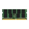

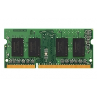
Kingston 8GB (1x8GB) 2400MHz DDR4 ECC 260-Pin CL17 SODIMM Server
Memory Module
... FBGA components. The SPD is programmed to JEDEC standard latency DDR4-2400 timing of 17-17-17 at 1.2V. Each 260-pin SODIMM uses gold contact fingers.FeaturesPower Supply: VDD=1.2VVDDQ = 1.2VVPP - 2.5VVDDSPD=2.2V to 3.6VFunctionality and operations comply with the DDR4 SDRAM datasheet16 internal banksBank Grouping is applied, and CAS to CAS latency (tCCD_L, tCCD_S) for the banks in the same or different bank group accesses are availableData transfer rates: PC4-2400, PC4-2133, PC4-1866, PC4-1600Bi-directional Differential Data Strobe8-bit pre-fetchBurst Length (BL) switch on-the-fly BL8 or BC4(Burst Chop)Supports ECC error correction and detectionOn-Die Termination (ODT)Temperature sensor with integrated SPDThis product is in compliance with the RoHS directivePer DRAM Addressability
is supportedInternal Vref DQ level generation is availableWrite CRC is supported at all speed gradesCA parity (Command/Address Parity) mode is supportedRoHS Compliant and Halogen-FreeExtra InfoMemory Size: 8192MBModule Size: 8192MBMemory Type: DDR4Memory Package: SO-DIMMPin Configuration: 260 pinsMain Colour: Green
is supportedInternal Vref DQ level generation is availableWrite CRC is supported at all speed gradesCA parity (Command/Address Parity) mode is supportedRoHS Compliant and Halogen-FreeExtra InfoMemory Size: 8192MBModule Size: 8192MBMemory Type: DDR4Memory Package: SO-DIMMPin Configuration: 260 pinsMain Colour: Green
%202400MHz%20DDR4%20ECC%20260-Pin%20CL17%20SODIMM%20Server%20Memory%20Module "Pin It")
Product Description
Reviews/Comments
Add New
Intelligent Comparison
Archived Product

Kingston 8GB (1x8GB) 1600MHz DDR3 240-Pin CL11 DIMM PC Memory Module MyMemory
£39.99
Archived Product
Kingston 4GB 1600MHz DDR3 Non-ECC 204 Pin CL11 SO-DIMM Laptop Memory Module MyMemory
£45.99
Archived Product

Kingston 4GB 1600MHz DDR3 240 Pin CL11 DIMM PC Memory Module MyMemory
£45.99
Archived Product
Kingston 4GB 1600MHz DDR3L Non-ECC 204 Pin CL11 SO-DIMM Laptop Memory Module MyMemory
£45.99
Archived Product

Kingston Value RAM 8GB 1600MHz DDR3 ECC 240 Pin CL11 DIMM PC Memory Module MyMemory
£88.99
Archived Product

Kingston 4GB 1600MHz DDR3L 240 Pin CL11 DIMM PC Memory Module MyMemory
£45.99
Archived Product

Kingston ValueRAM 16GB (2x8GB) 1600MHz DDR3 Non-ECC 240-Pin CL11 DIMM PC Memory Module MyMemory
£103.96
Archived Product

Kingston ValueRAM 16GB (2 X 8GB) 1600MHz DDR3 Non-ECC 204 Pin CL11 SO-DIMM Laptop Memory Module MyMemory
£102.99
 Denmark