-
Home
-
Contributors
-
International
-
Account
-
Information
More From Contributor
- white, with a black PCB. So your rig can reflect your style & you can show it off with pride. It is 100 per cent tested & LAN-ready plus it is backed by free technical support. Automatic Overclocking Reach faster speeds & higher capacities by just installing the memory, no adjustments in BIOS needed. Available in Kits of Two Does your system have enough memory to get you into the game? Kits are available to max out your systems with high-performance goodness. Find the Colour that Matches Your System Make sure your system looks as good as it performs. With multiple colours to choose from
- black, blue, red & white, the Hyper X Fury is sure to go with that custom case mod you have been working on. Compatible with Intel & AMD Platforms No matter if you are an Intel or AMD gamer, the Hyper X Fury is ideal for you. To make sure it works, Hyper X Fury has been tested with popular brands of motherboards. Free Technical Support When you spend that much time building your ideal system, make sure your memory lasts. With Hyper X memory you get free technical support to help you out if you are in a tight spot. From Hyper X, A Leader in e Sports Hyper X supports some of the best gaming teams in the world. While you might not be a pro yet, you can certainly game with the same equipment they do. Key Features
- Tested with good brands of motherboards
- Easy to install
- features plug-&-play functionality
- Automatic overclocking
- reach faster speeds & higher capacities by installing the memory, no adjustments in BIOS needed
- Reliable
- 100% factory tested
- Guaranteed
- free technical support ...
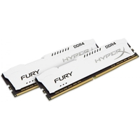
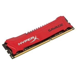
HyperX FURY 8GB (2x4GB) 1333MHz DDR3 Non-ECC CL9 DIMM PC Memory Module
- White
at lower then TCASE 85°C, 3.9us at 85°C TCASE. 95°C Asynchronous Reset PCB: Height 1.18 inch (30mm), single sided component Extra Info Memory Size: 8192MB Module Size: 4096MB Memory Type: DDR3 Memory Package: DIMM Pin Configuration: 240 pins Main Colour: White
This page now acts as a permanent archive for this product. Add more information using the comments box below to ensure it can still be found by future generations.
Use our search facility to see if it is available from an alternative contributor.
- External links may include paid for promotion
- Availability: Out Of Stock
- Supplier: MyMemory
- SKU: 14905
Product Description
. .. DDR3 FBGA components per module. Total kit capacity is 8GB. Each module kit has been tested to run at DDR3-1333 at latency timing 9-9-9 at 1.5V. Features JEDEC standard 1.5V (1.425V ~ 1.575V) Power Supply VDDQ = 1.5V (1.425V ~ 1.575V) 667 M Hz f CK for 1333 Mb/sec/pin 8 independent internal bank Programmable CAS Latency: 9, 8, 7, 6 Programmable Additive Latency: 0, CL
- 2, or CL
- 1 clock 8-bit pre-fetch Burst Length: 8 (Interleave without any limit, sequential with starting address '000' only), 4 with t CCD = 4 which does not allow seamless read or write [either on the fly using A12 or MRS] Bi-directional Differential Data Strobe Internal (self) calibration: Internal self calibration through ZQ pin (RZQ: 240 ohm ± 1%) On Die Termination using ODT pin Average Refresh Period 7.8us at lower then TCASE 85°C, 3.9us at 85°C TCASE. 95°C Asynchronous Reset PCB: Height 1.18 inch (30mm), single sided component Extra Info Memory
Size: 8192MB Module
Size: 4096MB Memory Type: DDR3 Memory Package: DIMM Pin Configuration: 240 pins Main
Colour: White
Reviews/Comments
Add New
Intelligent Comparison
Price History
Vouchers
Jargon Buster
Supplier Information
Flash Memory
Mobile Accessories
Computer devices and peripherals
Electronic Toys and Gadgets
And much more...
Live Chat is available
Delivery is usually within 3-5 days via royal mail.
Orders are dispatched from Jersey within 24 hours.
Lines are open 10am to 5pm Monday to Friday - 0871 873 7899 (Call are charged at 10p per minute)


 United Kingdom
 France
 Germany
 Netherlands
 Sweden
 USA
USA
 Italy
Italy
 Spain
Spain






 Denmark