
 United Kingdom
 France
 Germany
 Netherlands
 Sweden
 USA
USA
 Italy
Italy
 Spain
Spain
More From Contributor
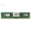
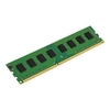


Kingston 8GB DDR4 2400MHz ECC DIMM Memory
Power Supply VDD = 1.2VVDDQ = 1.2VVPP = 2.5VVDDSPD = 2.25V to 2.75VFunctionality and operations comply with the DDR4 SDRAM datasheet16 internal banksBank Grouping is applied and CAS to CAS latency (tCCD_L tCCD_S) for the banks in the same or different bank group accesses are availableData transfer rates PC4-2400 PC4-2133 PC4-1866 PC4-1600Bi-Directional Differential Data Strobe8 bit pre-fetchBurst Length (BL) switch on-the-fly BL8 or BC4(Burst Chop)Supports ECC error correction and detectionOn-Die Termination (ODT)Temperature sensor with integrated SPDThis product is in compliance with the RoHS directive.Per DRAM Addressability is supportedInternal Vref DQ level generation is availableWrite CRC is supported at all speed gradesCA parity (Command/Address Parity) mode is supported..

Product Description
Reviews/Comments
Add New
Intelligent Comparison
Archived Product
Kingston 16GB DDR4 2666MHz ECC DIMM Memory Laptops Direct
£69.97
Archived Product

Kingston 4GB DDR3L 1600MHz Non-ECC DIMM Memory Laptops Direct
£33.97
Archived Product

Kingston 32GB DDR4 2666MHz DIMM Memory Laptops Direct
£105.56
Archived Product
Kingston - 16GB - DDR4 - 2666MHz - ECC DIMM Memory Laptops Direct
£129.00
Archived Product

Kingston 8GB DDR3 1600MHz Non-ECC DIMM Desktop Memory Laptops Direct
£59.98
Archived Product

Kingston 8GB DDR3L 1600MHz Non-ECC DIMM Desktop Memory Laptops Direct
£59.98
Archived Product

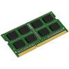
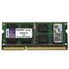
Kingston 8GB DDR3 1600MHz Non-ECC SO-DIMM Laptop Memory Laptops Direct
£63.97
Archived Product

Kingston 4GB DDR3 1600MHz Non-ECC DIMM Desktop Memory Laptops Direct
£33.97
 Denmark